


Samsung Electronics Starts Mass Production of '3D V-NAND' by Operating Largest Semiconductor Line in Pyeongtaek
 Published2017.07.04 14:15
Expansion of Pyeongtaek Line 1 Begins, Total Investment of 30 Trillion Won Expected by 2021
Samsung Electronics is pursuing an investment of over 37 trillion won, including the full-scale operation of its Pyeongtaek semiconductor line and the expansion of its semiconductor and display production lines.
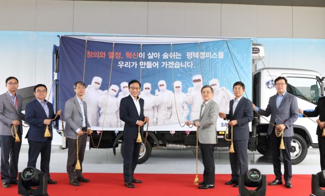
Samsung Electronics held a product shipment ceremony at its Pyeongtaek semiconductor complex on the 4th and began mass production of state-of-the-art 3D V-NAND. The shipment ceremony on this day was attended by key executives and about 100 employees, including CEO and Vice Chairman Kwon Oh-hyun, Semiconductor General Manager Kim Ki-nam, and heads of each business unit in the DS division.
In his congratulatory remarks, Samsung Electronics Executive Vice Chairman and CEO Kwon Oh-hyun stated, "The Pyeongtaek Semiconductor Complex is a new challenge for the future of Samsung Electronics' semiconductor business," adding, "I express my gratitude to the employees and partner companies who successfully prepared for this first challenge."

Samsung Electronics’ Pyeongtaek semiconductor line is the world’s largest single line; construction began in May 2015 and was completed in two years, with an average of about 12,000 workers deployed to the construction site daily.
The products manufactured at the Pyeongtaek semiconductor line are state-of-the-art 4th generation 64-layer V-NAND products, and starting with this operation, Samsung Electronics plans to continuously expand its production facilities for memory
The plan is to strengthen market competitiveness.
Samsung Electronics plans to expand its production capacity by actively investing in domestic and international production bases and actively respond to the growing demand for semiconductors from global IT customers. With plans to expand the Pyeongtaek Line 1, which recently began operations, the total investment scale, including existing investments, is expected to reach 30 trillion won by 2021.
Samsung Display Considers Construction of New OLED Complex Infrastructure in Asan, South Chungcheong Province
Samsung Electronics plans to invest 6 trillion won not only in Pyeongtaek but also in its Hwaseong plant to secure new lines optimized for advanced infrastructure such as EUV, as part of its strategy to prepare for the future semiconductor market. In addition, Samsung Electronics is considering building an additional semiconductor line in Xi'an, China. The Xi'an semiconductor line, completed in 2014, is currently operating at 100% capacity, and the strategy is to respond to the Chinese market, the largest consumer of NAND flash, by constructing additional lines to secure 'economies of scale'.
Meanwhile, Samsung Display is considering constructing infrastructure for a new OLED complex in the Asan region of South Chungcheong Province. Samsung Display had decided to begin construction of Asan Complex 2 by 2018.
We are planning investments in land and infrastructure facilities to comply with the complex construction agreement with Chungcheongnam-do and to respond flexibly to rapidly changing market conditions.
Through this large-scale investment by Samsung Electronics and Samsung Display, the establishment of an advanced components cluster spanning Giheung, Hwaseong, and Pyeongtaek in Gyeonggi Province and Asan in Chungcheong Province is expected to foster co-growth with the domestic equipment and materials industries, as well as revitalize the downstream industrial ecosystem, thereby expanding the demand for high-skilled technical personnel in R&D and services.
Comments
Related news
3D NAND on the Rise, Finding Processes and Materials to Solve Stacking Challenges
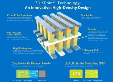
With 3D NAND supply volumes expected to surpass 2D NAND this year, interest is growing in the processes and materials required for stacking 3D NAND. On the 18th, the Semiconductor Electronic Materials Technology Conference (SMC, Strategic Materials Conference), hosted by the International Semiconductor Equipment and Materials Institute, was held under the theme "Scaling Challenges-The Future of Materials," discussing semiconductor material challenges for next-generation memory, market outlook for semiconductor materials, key process material technologies, and DRAM prospects. Sung-hyun Hong, Executive Director of Ram Research Korea, who presented, addressed the problems that arise as 3D NAND is stacked: "As the number of layers increases, the height becomes extremely high. If the structure is not harmonious, stress changes become severe. When stress becomes severe, the wafer bends, making handling difficult in subsequent processes."
2017.05.22by 김지혜 기자
Samsung Electronics Expands 4th Generation V-NAND Lineup by Overcoming Limitations of 3D Stacking Technology
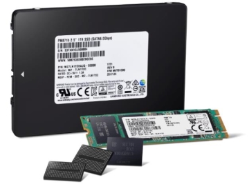
Samsung Electronics is ramping up mass production of "4th generation (64-layer) 256-gigabit (Gb) 3-bit V-NAND flash" that implements world-leading performance and high reliability, expanding its 4th generation V-NAND lineup across all NAND products for servers, PCs, and mobile applications. Following the supply of 4th generation 256Gb V-NAND-based SSDs to global B2B customers that began last January, Samsung Electronics plans to expand 4th generation V-NAND to mobile eUFS, consumer SSDs, and memory cards, while increasing monthly production share to over 50% within this year to address growing global customer demand. Three innovative technologies—"ultra-high integration cell structure and process," "ultra-high-speed operation circuit design," and "ultra-high reliability CTF thin film formation"—are applied to the 4th generation (64-layer) V-NAND, achieving over 30% improvement in speed, productivity, and power efficiency compared to 3rd generation (48-layer) products.
2017.06.15by 김지혜 기자
Western Digital Develops Next-Generation 96-Layer Vertically Stacked 3D NAND Technology
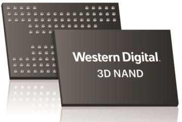
Western Digital announced the successful development of 'BiCS4,' its next-generation 96-layer vertical stacked 3D NAND technology. BiCS4, jointly developed with Toshiba, Western Digital's technology and manufacturing partner, will initially be produced as 256Gb (gigabit) chips, and will subsequently be shipped in various capacities including single 1Tb (terabit) chips. It will be offered in both 3-bit per cell (TLC) and 4-bit per cell (QLC) architectures, with sampling for OEM customers planned for the second half of 2017 and pilot production slated to begin during 2018.
2017.06.29by 신윤오 기자

Intel Unveils Next-Generation 'Core Ultra Series 3' and vPro Platform for Enterprise PCs
Intel has officially unveiled the "Intel Core Ultra Series 3" for next-generation enterprise PCs and the latest vPro platform, addressing a wide range of demands from enterprise notebooks to high-performance workstations.
2026.03.26by 배종인 기자

ROHM Launches ESD Protection Diode Compatible with High-Speed Interfaces of 10Gbps or Higher
Semiconductor specialist ROHM has developed the 'RESDxVx series' of ESD (electrostatic discharge) protection diodes capable of responding to next-generation high-speed data communication environments exceeding 10Gbps, simultaneously enhancing both signal quality maintenance required in high-speed interfaces and IC protection performance.
2026.03.26by 배종인 기자











