


Lattice Nexus, Low-Power FPGA Platform for Edge AI Unveiled
 Published2019.12.11 11:11
CrossLink-NX supports 170-bit memory per logic cell
Developed with Samsung Electronics' 28nm FD-SOI technology
On the 11th, Lattice Semiconductor announced its new low-power FPGA platform, 'Lattice Nexus,' and the first device based on it, 'CrossLink-NX.'
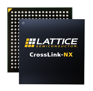
Crosslink-NX (Photo = Reted Semiconductor)
The Lattice Nexus platform is designed for embedded developers looking to implement AI applications at the edge and was developed using Samsung Electronics' 28nm FD-SOI (Fully-Depleted Silicon-On-Insulator) process technology. This technology offers 50% less transistor leakage than bulk CMOS. With this, Lattice has become Samsung Electronics Foundry's first FPGA customer.
It also released 'Lattice Radiant 2.0', a software tool for FPGA design. Because the design flow, from the design planning stage to IP porting, implementation, bitstream generation, and downloading bitstreams to the FPGA, is automated, even FPGA inexperienced developers can easily develop.
CrossLink-NX consumes 75% less power than equivalent FPGAs
CrossLink-NX, the first FPGA device based on the Nexus platform, features low power, a small form factor, reliability, and performance characteristics required for developing AI solutions for embedded vision systems as well as communications, computing, industrial, automotive, and consumer systems.
Compared to competing FPGA products in the same class, it consumes up to 75% less power and has a Soft Error Rate (SER) up to 100 times lower. It also supports various high-speed I/O including MIPI, PCIe, and DDR3 memory.
CrossLink-NX also supports instant-on functionality to support industrial applications where long system boot times are critical. I/O configuration is possible within 3ms, and full device configuration is possible within 15ms.
To enable efficient AI inference on edge devices, it supports 170 bits of memory per logic cell, which is twice as much as the previous generation device. Available in a 6×6mm form factor, CrossLink-NX is up to 1/10 the size of competing FPGA products in its class.
Lattice provides not only Radiant 2.0 but also IP core libraries such as MIPI D-PHY, PCIe, SGMII, and OpenLDI, as well as demo materials for common embedded vision applications such as 4:1 image sensor aggregation.

(Photo by Reporter Lee Su-min)
"FPGAs support the power-efficient performance required by new technologies such as AI inference at the edge and sensor management," said Yign Jen Chen, Director of Business Development for Lattice Asia Pacific. "The Lattice Nexus platform, which enhances the parallel processing and reprogramming capabilities of FPGAs, will accelerate Lattice's future product launch speed."
He added, “The Lattice Nexus platform provides an easy-to-use solution stack targeting rapidly growing core applications,” and “supports users unfamiliar with FPGA design to easily and quickly develop their own systems.”
Comments
Related news

Lattice Begins Samples of FPGAs for Embedded Vision Systems
Lattice announced a CrossLink Plus FPGA product family for MIPI D-PHY-based embedded vision systems. CrossLink Plus features embedded flash memory hardware-based MIPI D-PHY and high-speed I/O for instant-on panel displays, and is a low-power FPGA that enables on-device programming. Ready-to-use IP and reference designs are also provided.
2019.10.15by 이수민 기자
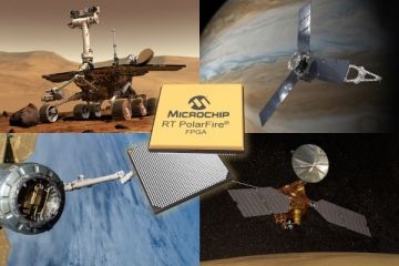
Microchip Launches Low-Power Radiation-Resistant FPGA for Space
Space applications are increasingly transmitting processed data rather than simple raw data. Additionally, to maximize the utilization of limited downlink bandwidth, they require increasingly superior computing performance. Microchip has launched a radiation-hardened PolarFire FPGA to address this need. It delivers 1.5x performance, 3x logic elements, and SERDES bandwidth in applications requiring up to 5x computing throughput. It provides 6x higher embedded SRAM and withstands TID exposure exceeding 100kRad, which is commonly encountered in the majority of satellites in Earth orbit and numerous deep space missions.
2019.10.24by 이수민 기자
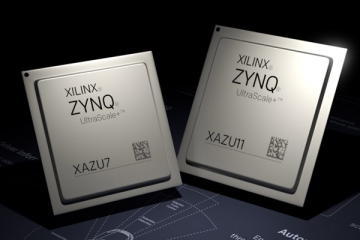
Xilinx Expands Battlefield FPGA Market with Launch of 7EV and 11EG
Xilinx has launched the 7EV and 11EG, 16nm-based XA Zynq UltraScale+ MPSoCs that have obtained AEC-Q100 automotive certification. The 7EV and 11EG commonly provide over 650,000 programmable logic cells and approximately 3,000 DSP slices. The 7EV includes a video codec for H.264/H.265 encoding and decoding, while the 11EG offers 32 12.5Gb/s transceivers and 4 PCIe3 x16 blocks. The XA Zynq UltraScale MPSoC portfolio integrates Xilinx programmable logic along with a processing system based on a 64-bit quad-core Arm Cortex-A53 and dual-core Arm Cortex-R5, certified to ASIL-C level in the low-power domain.
2019.11.14by 이수민 기자

Intel Unveils Next-Generation 'Core Ultra Series 3' and vPro Platform for Enterprise PCs
Intel has officially unveiled the "Intel Core Ultra Series 3" for next-generation enterprise PCs and the latest vPro platform, addressing a wide range of demands from enterprise notebooks to high-performance workstations.
2026.03.26by 배종인 기자

ROHM Launches ESD Protection Diode Compatible with High-Speed Interfaces of 10Gbps or Higher
Semiconductor specialist ROHM has developed the 'RESDxVx series' of ESD (electrostatic discharge) protection diodes capable of responding to next-generation high-speed data communication environments exceeding 10Gbps, simultaneously enhancing both signal quality maintenance required in high-speed interfaces and IC protection performance.
2026.03.26by 배종인 기자











