



Understanding Noise Levels by Switching Regulator Topology
 Published2020.10.16 09:00
You need to understand which terminal has the highest noise.
You can plan your filters in advance and secure the space you need.
There are many different switching regulator topologies. The most widely used is the traditional step-down converter, also known as the buck converter. There are also lesser-known switch-mode DC/DC converters, such as the zeta topology.
They can be divided into basic topologies and extended topologies. The basic topology is a non-isolated switching regulator that uses only two switches, one inductor, and two capacitors. In other words, it is a switching regulator that is not electrically isolated. Buck converters, boost converters, and inverting buck-boost topologies belong here.
All other topologies require additional components. For example, the SEPIC converter requires a coupling capacitor and a secondary inductor. Unlike non-isolated switching regulators, there are also several regulators that use a transformer to provide galvanic isolation.
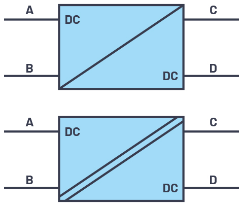
Circuit design engineers sometimes refer to power supplies as black boxes or 4-pole devices, each with two input lines and two output lines. [Figure 1] shows a block diagram of a DC/DC converter. The one above is a DC/DC converter without galvanic isolation, and the one below is a converter with galvanic isolation.
No noise information is available regarding the terminals here. The behavior of the two-port network terminals varies depending on the switching regulator topology. [Figure 2] shows the ADP2441 from Analog Devices (ADI) as a general-purpose step-down converter for industrial applications.
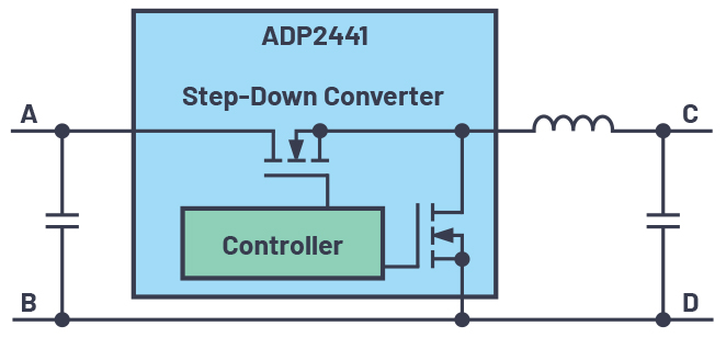
This converter converts 24 V input to 3.3 V output. This topology is very noisy because it generates pulsed current at the input. When the high-side switch of ADP2441 is on, current flows to terminal A.
When this switch is off, no current flows through node A. However, there is almost no noise on the output side C. This is because the inductor in the output path prevents pulse-like current from being generated at the output terminal.
[Table 1] is intended to help system design engineers understand the basic operation of a switching regulator. This table summarizes the major switching regulator topologies in common use.
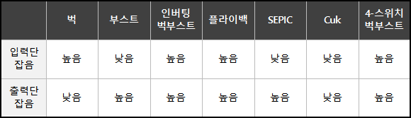
Noise levels at input and output by topology
The first row shows whether the noise level at the input is high or low. That is, it indicates the noise level at terminals A and B of the two-port network.
The second row indicates whether the noise level at the output is high or low, that is, the noise level at terminals C and D of the two-port network.
Conductive noise in switching regulator circuits can be significantly reduced by additional filtering, for example, a separate LC filter. This method can overcome the weaknesses shown in Table 1.
However, system design engineers need to understand which DC/DC converters have particularly high noise at which terminals, so that they can design appropriate filters in advance during the design phase and reserve the necessary space for them.
This article is a summary of the article titled “Noise from Different Switching Regulator Topologies” by Frederik Dostal, Power Management FAE at Analog Devices.
Comments
Related news
Things to Know Before Buying a Switch Mode Power Supply
SMPS switches at a frequency that is fixed, variable, or synchronized to an external clock. The physical size of the device varies depending on the switching frequency value, and accordingly, the cost of capacitors and inductors in the power supply also varies. Recently, there is a trend toward shifting to higher switching frequency values for more compact and cost-effective circuit design.
2020.06.23by 이수민 기자
.png)
Buck/boost controllers for dual-battery vehicles now available
Mouser Electronics announced that it supplies ADI's LT8228 and LTC7871 bidirectional buck/boost controllers, which provide bidirectional voltage/current regulation and bidirectional reverse current protection capabilities. The two controllers operate in either buck or boost mode as needed and are suitable for 48V/12V dual battery automotive systems.
2020.08.07by 명세환 기자

"DC/DC converter, peripheral circuit design is important"
Electronic products operating on wall outlet power require an AC/DC converter to convert AC 220V to DC. This is because most ICs operate only on DC. DC/DC converters are equally important. The numerous ICs used in electronic products each have different operating voltages and voltage precision requirements, as unstable power supply voltages can cause IC malfunctions and characteristic degradation.
2020.08.21by 이수민 기자

Intel Unveils Next-Generation 'Core Ultra Series 3' and vPro Platform for Enterprise PCs
Intel has officially unveiled the "Intel Core Ultra Series 3" for next-generation enterprise PCs and the latest vPro platform, addressing a wide range of demands from enterprise notebooks to high-performance workstations.
2026.03.26by 배종인 기자

ROHM Launches ESD Protection Diode Compatible with High-Speed Interfaces of 10Gbps or Higher
Semiconductor specialist ROHM has developed the 'RESDxVx series' of ESD (electrostatic discharge) protection diodes capable of responding to next-generation high-speed data communication environments exceeding 10Gbps, simultaneously enhancing both signal quality maintenance required in high-speed interfaces and IC protection performance.
2026.03.26by 배종인 기자











