



Onsemi Signs MOU with Pennsylvania State University for SiC Research
 Published2023.05.19 12:08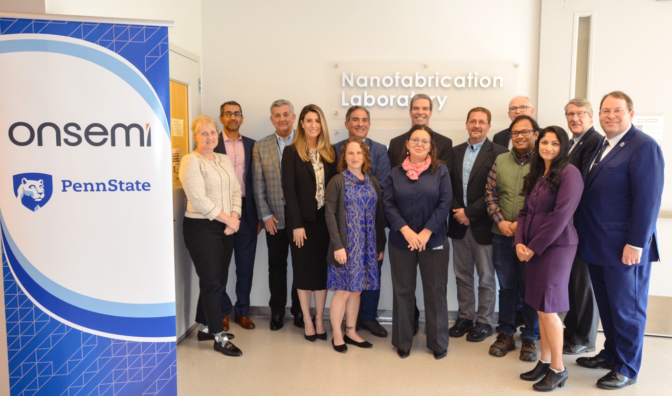
Onsemi signs MOU with Pennsylvania State University for SiC research in the US (Photo: Onsemi)
Silicon carbide (SiC) is essential for improving the efficiency of electric vehicles (EVs), EV charging, and energy infrastructure, and contributes to the decarbonization of the global economy. While academic research on SiC in the United States made significant progress in the late 1990s and early 2000s, its scale has since declined. Recent agreements are signaling a revitalization of SiC crystal research in the United States.
Onsemi announced on the 19th that it has signed a memorandum of understanding (MOU) with Pennsylvania State University (Pennsylvania State University) for a strategic collaboration worth $8 million (approximately 10.6 billion won) to promote silicon carbide (SiC) research.
This collaboration will establish the Onsemi Silicon Carbide Crystal Center (SiC3) at Penn State's Materials Research Institute (MRI). Onsemi plans to provide SiC3 with $800,000 (approximately KRW 1 billion) annually for the next 10 years.
In addition to conducting SiC research in SiC3, Penn State and Onsemi are raising awareness of the growing demand for technical jobs in the semiconductor industry. This is part of an effort to increase the U.S. share of semiconductor manufacturing, including collaboration on workforce development initiatives such as internships and co-op programs and inclusion of research in SiC and wide-bandgap crystals in Penn State's curriculum.
These partnerships with Penn State University are dedicated to promoting STEAM (Science, Technology, Engineering, Arts, and Mathematics) education, from supporting K-12 students in underserved communities to university collaborations that support the development of the current and future workforce.
Lora Weiss, vice president for research at Penn State, said the collaboration between Penn State and Onsemi was a perfect fit given each institution's proven strengths.
“We have world-class nanofabs and characterization facilities that support research on thin films, SiC, and other materials used in semiconductors and other technologies,” said Laura, vice president for research. “These complementary capabilities between ON Semiconductor and Penn State will have a significant impact on research and development, economic growth, and workforce development.”
“Penn State is uniquely positioned to rapidly establish a SiC crystal growth research program,” said Pavel Freundlich, chief technology officer of ON Semiconductor’s Power Solutions Group. “The university brings a broad range of capabilities based on its current materials research, wafer processing capabilities at its nanofab facility, and a comprehensive suite of world-class metrology instruments.”
“Over the next decade, this collaboration will make Penn State the nation’s leading resource for semiconductor crystal science and workforce development,” said Justin Schwartz, Penn State’s vice president for research and development, and Priya Babu, Penn State’s senior director of corporate and industry engagement.“This would not have been possible without the relationship-building efforts of our (aboo) colleagues, the technical expertise of Joshua Robinson, Professor of Materials Science and Engineering, and the Onsemi team,” he said.
“Penn State’s expansion of our curriculum to offer specialized courses in SiC and wide-bandgap technologies is a key step toward achieving ON Semiconductor’s strategic workforce development goals,” said Scott Allen, ON Semiconductor’s vice president of university relations. “This expansion will help us achieve the U.S. semiconductor workforce goals outlined in the recently signed CHIPS and Science Act.”

Comments
Related news
.jpg)
Mouser supplies ON Semi EliteSiC product family
Mouser Electronics supplies onsemi's EliteSiC silicon carbide (SiC) solution product line.
2023.04.03by 배종인 기자

ON Semi, Long-term Supply of SiC Device Zicers
onsemi, a leading company in intelligent power and sensing technology, contributes to extending the driving range of smart electric vehicles by supplying silicon carbide devices to ZEEKR, a premium electric mobility brand.
2023.04.26by 배종인 기자
ON Semi Launches Next-Generation 1,200V SiC M3S Device
ON Semiconductor, a leading company in intelligent power and sensing technology, has launched next-generation silicon carbide (SiC) devices, which are expected to contribute to improved efficiency in electric vehicle and energy infrastructure applications.
2023.05.10by 배종인 기자

Intel Unveils Next-Generation 'Core Ultra Series 3' and vPro Platform for Enterprise PCs
Intel has officially unveiled the "Intel Core Ultra Series 3" for next-generation enterprise PCs and the latest vPro platform, addressing a wide range of demands from enterprise notebooks to high-performance workstations.
2026.03.26by 배종인 기자

ROHM Launches ESD Protection Diode Compatible with High-Speed Interfaces of 10Gbps or Higher
Semiconductor specialist ROHM has developed the 'RESDxVx series' of ESD (electrostatic discharge) protection diodes capable of responding to next-generation high-speed data communication environments exceeding 10Gbps, simultaneously enhancing both signal quality maintenance required in high-speed interfaces and IC protection performance.
2026.03.26by 배종인 기자











