



Applied Materials Targets 'Memory Wall' in AI Era...Presents Solutions Across D-RAM, HBM, and Packaging
 Published2026.08.31 16:56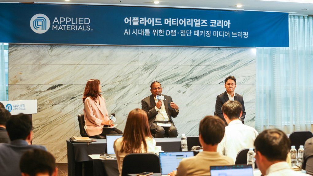
재료·장비·공정·패키징 통합 최적화, 차세대 AI 반도체 성능 향상
고객사 생산능력 확대 맞춘 장기 공급망 협력 등 공동 개발 강화
인공지능(AI) 시대 반도체 경쟁의 승패가 ‘연산’보다 ‘데이터 이동’에 달리고 있다. AI 모델이 거대화될수록 전력 소모와 메모리 병목이 시스템 성능을 제한하는 핵심 과제로 떠오르는 가운데, 어플라이드 머티어리얼즈(Applied Materials)가 D램 소자 혁신부터 HBM(고대역폭메모리), 하이브리드 본딩, 공동광학패키징(CPO)까지 아우르는 통합 포트폴리오를 앞세워 차세대 AI 반도체의 성능·전력 효율·생산성 향상을 지원하겠다는 전략을 제시했다.
어플라이드 머티어리얼즈 코리아는 31일 서울 오크우드 프리미어 코엑스에서 ‘AI 시대를 위한 D램·첨단 패키징 미디어 브리핑’을 열고 AI 확산에 따른 반도체 산업의 구조적 변화와 기술 로드맵을 소개했다.
이날 행사에는 박광선 어플라이드 머티어리얼즈 코리아 대표와 무쿤드 스리니바산(Mukund Srinivasan) 어플라이드 머티어리얼즈 그룹 부사장이 참석했다.
행사의 핵심 메시지는 분명했다. AI 시대에는 더 이상 개별 칩 성능만으로 경쟁할 수 없으며, 로직과 메모리, 패키징을 하나의 시스템으로 최적화해야 한다는 것이다.
무쿤드 부사장은 AI 산업이 직면한 가장 큰 과제로 ‘에너지 효율’과 ‘생산능력 확대’를 꼽았다. AI 모델의 연산량이 폭증하면서 데이터 이동에 소비되는 전력이 급증하고 있으며, 이를 해결하기 위한 산업 전반의 해법이 바로 ‘3D 스케일링’이라고 설명했다. 로직에서는 GAA(게이트올어라운드)와 같은 3차원 구조가, 메모리에서는 HBM과 같은 적층 기술이, 패키징에서는 2.5D·3D 통합 기술이 각각 핵심 역할을 하고 있다는 분석이다.
어플라이드는 이러한 변화 속에서 단순 장비 공급업체가 아닌 ‘기술 플랫폼 제공자’ 역할을 강조했다. 특히 3D 스케일링을 구현하기 위한 핵심 요소로 신소재, 선택적 증착·식각 공정, 옹스트롬 수준의 공정 제어 및 계측, 공정 통합 최적화 등 네 가지 혁신 축을 제시했다. 로직 공정이 2,000단계 이상, 메모리 공정이 1,200단계 이상으로 복잡해지는 상황에서 개별 장비 성능뿐 아니라 전체 공정의 연결성과 공동 최적화가 중요해지고 있다는 설명이다.
특히 AI 반도체의 최대 난제로 꼽히는 ‘메모리 장벽(Memory Wall)’ 해결 전략이 주목을 받았다. AI 프로세서 성능 향상 속도가 메모리 발전 속도를 앞지르면서 이제는 얼마나 빠르게 데이터를 공급하느냐가 시스템 성능을 좌우하고 있다. 이에 따라 어플라이드는 선단 로직에서 검증된 기술을 D램으로 확장하는 데 집중하고 있다. 에피택시, 금속배선, CMP 등 로직용 핵심 기술을 D램 주변회로에 적용해 속도와 전력 효율을 동시에 높이겠다는 전략이다.
D램 기술 로드맵과 관련해서는 CBA(CMOS Bonded Array), 4F² 수직 트랜지스터 구조, 장기적으로는 3D D램 개발까지 다양한 기술 진화 방향을 제시했다.
무쿤드 부사장은 “3D D램이 EUV를 완전히 대체하는 것은 아니지만, EUV 사용량을 크게 줄일 수 있다”며 “개별 소재와 공정 기술에는 자신감을 갖고 있으며, 남은 과제는 이를 효과적으로 통합하는 것”이라고 말했다.
HBM과 첨단 패키징 분야에서는 하이브리드 본딩이 핵심 키워드로 제시됐다.
기존 마이크로범프 방식은 칩 간 간격의 물리적 한계를 갖지만, 하이브리드 본딩은 사실상 다이 간 거리를 제로 수준까지 줄여 I/O 밀도와 전력 효율, 대역폭을 획기적으로 높일 수 있다.

어플라이드는 이를 위해 하이브리드 본딩 시스템 ‘키넥스(Kinex)’와 CMP, 구리 증착, 계측·검사 솔루션을 포함한 광범위한 기술 포트폴리오를 확보했다고 밝혔다.
또한 공동광학패키징(CPO)에 대해서도 높은 기대감을 나타냈다.
CPO는 패키지 내부 일부 전기 배선을 광 신호 기반 연결로 대체하는 기술로, 차세대 AI 데이터센터의 핵심 기술로 평가받는다.
어플라이드는 광 신호 전송을 위한 웨이브가이드용 신소재와 관련 공정 기술 개발을 진행 중이며, 하이브리드 본딩 기술 역시 CPO 구현의 기반 기술로 보고 고객사들과 긴밀히 협력하고 있다고 설명했다.
한국 시장의 전략적 중요성도 강조됐다.
박광선 대표는 삼성전자와 SK하이닉스가 글로벌 AI 메모리 생태계의 중심에 있다고 평가하며, 한국의 중요성이 앞으로 더욱 커질 것으로 전망했다.
그는 “HBM과 첨단 메모리 시장에서 한국 기업들이 차지하는 위상은 매우 크다”며 “AI 시대가 본격화될수록 한국은 메모리뿐 아니라 첨단 패키징과 선단 로직까지 아우르는 전략적 거점으로 부상할 것”이라고 말했다.
어플라이드는 이를 지원하기 위해 고객사 생산능력 확대에 맞춘 장기 공급망 협력, 글로벌 생산거점 확대 지원, 차세대 패키징 공동 개발을 강화하고 있다.
또한 EPIC(Equipment and Process Innovation and Commercialization) 플랫폼을 통해 고객사, 대학, 파트너 기업들과 공동 연구개발 체계를 구축하고 있다.
현재 EPIC 프로젝트에는 삼성전자와 SK하이닉스를 포함한 주요 반도체 기업들이 참여하고 있으며, 실리콘밸리 EPIC 센터와 한국 오산의 ACC Korea를 연결해 연구개발부터 양산 검증까지의 시간을 단축한다는 계획이다.
결국 어플라이드 머티어리얼즈가 제시한 AI 시대 해법은 ‘더 많은 트랜지스터’가 아니라 ‘더 효율적인 데이터 이동’에 있다.
D램, HBM, 첨단 패키징, 광연결 기술을 하나의 연속된 혁신 과제로 묶고 재료·장비·공정·패키징을 통합 최적화함으로써 AI 성능을 높이겠다는 것이다.

Comments
Related news
Applied Sponsors 'Our Stream Guardians' for 6th Year... Expands to Downtown Streams in Seoul
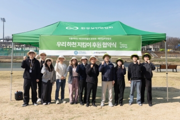
Applied Materials Korea has entered into an agreement with the Environmental Practices Alliance and continues the river conservation activity "Our River Guardians" for the sixth consecutive year. This year, the initiative expands beyond the existing focus on rivers in the Gyeonggi region to include Seoul's Tancheon, Anyang Stream, and Bulguang Stream. Customized programs by river are operated, including EM soil ball deployment, invasive plant removal, and purification plant planting, with both in-person and non-contact programs involving students, families, and citizens. Over the past six years, approximately 20,000 participants have deployed about 435,000 EM soil balls, and improvements in water quality grades have been confirmed in some rivers.
2026.03.24by 배종인 기자
.jpg)
Applied Materials Announces Two Deposition Equipment Models for Sub-2nm GAA Processes
Applied Materials announced two deposition equipment types targeting sub-2nm GAA processes. The Precision selective nitride PECVD aims to reduce parasitic capacitance and leakage through STI structure protection, while the Endura Trillium ALD focuses on precisely forming metal gate stacks on silicon nanosheets. The company stated that both tools are being applied in sub-2nm processes at leading logic manufacturers. The announcement aligns with growing demand for fine structure control in the production of high-performance and high-efficiency chips for AI semiconductors.
2026.04.14by 배종인 기자
.jpg)
Applied Materials Acquires NEXX… Expanding Panel-Based Advanced Packaging Capabilities
Applied Materials has entered into a contract to acquire ASMPT's NEXX business division. This acquisition is interpreted as a strategic move to expand panel-level process capabilities through securing large-area advanced packaging deposition technology. As AI chip designs scale up and chiplet structures proliferate, the shift from conventional wafer-based to panel-based manufacturing is accelerating, and this move aligns with intensifying competition in related equipment and processes. The transaction is expected to close within several months, and the organization will be integrated into the existing semiconductor business division following the acquisition.
2026.05.07by 배종인 기자
Applied Materials and TSMC Strengthen Joint Research in Silicon Valley… Driving Development of Next-Generation Semiconductor Processes
Applied Materials and TSMC are strengthening their collaboration for next-generation semiconductor process technology development at the Silicon Valley EPIC Center. The two companies will jointly research materials engineering, equipment, and process integration technologies, focusing on reducing the transition time from initial technology verification to mass production. In particular, they plan to cooperate in solving advanced logic structure and process complexity challenges in response to increasing AI and high-performance computing demand. This collaboration is assessed as a case reflecting the industry-wide trend of expanding joint research foundations in the semiconductor sector.
2026.05.12by 배종인 기자
Broadcom Joins Applied EPIC… Pursuing AI Packaging Collaboration
Applied Materials announced Broadcom as an EPIC platform partner and will collaborate on developing advanced packaging technologies for AI systems. Broadcom will examine multi-chip interconnection and heterogeneous integration technologies based on Applied Materials' research and development facilities. As AI semiconductor performance enhancement expands beyond chip design to encompass a combination of packaging and process technologies, this collaboration demonstrates a joint development workflow between equipment and process companies and system design companies.
2026.05.21by 배종인 기자











